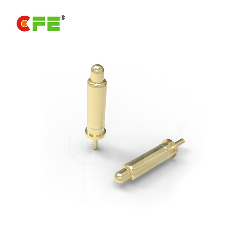
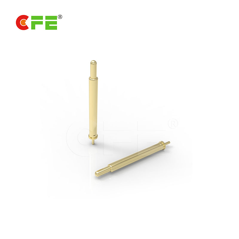
The spring loaded pins for pcb testing fixture is required to interface the main tester with the particular board being tested. It will have a main connector connected to the test instrument and a separate pin / probe / or “nail” wire removed from the connector, which is in contact with the desired node on the board.
The probe is held in place by a so-called substrate. This is the exact borehole to ensure that the probe remains in the correct position and the fixture is in contact with the desired node on the board.
 |
 |
| [MF310-1111] DIP spring loaded pins for pcb testing | [MF513-1111] Large spring contact probes pogo pins |
The plate is precisely held in place by the clamp and is pulled onto the spring loaded pins for pcb testing in contact with the plate. The plate can be pulled under the action of vacuum, or it can be mechanically realized.
Once the board assembly density is much lower, it is common to place a special ATE pad on the board to achieve a good connection. Nowadays, this very compact circuit board is not possible. But connected to the component pad. It is obviously more difficult to connect the solder and the parts themselves, but they can still be highly reliable. Typically, each spring is applied with a force of 100 to 200 g to ensure good contact. This obviously means that the total power required for all pins on the board may be significant. Sometimes it is necessary to support the board to make sure it does not bend too much as this may cause some fine surface mount components to rupture.
 |
 |
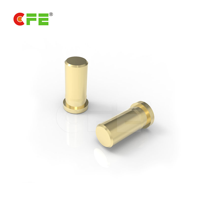
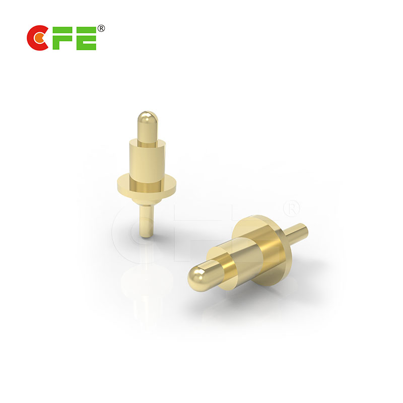
| [FF400-1110] Female terminal pins supplier | [BP94511] DIP PCB spring pogo probe pin |
The spring loaded pins for pcb testing are usually placed on a 0.1-inch matrix. Many new surface-mount IC packages require more fine spacing, and in order to achieve this, frequent use of adapters.
Contact Info: cfe@cfeconn.com


